产品展示
联系我们
联系人:麦女士
手机:+86 15270269218
电话:
Q Q:3136378118
邮箱:stodcdcs@gmail.com
地址:江西省九江市瑞昌市东益路23号赛湖农商城401号
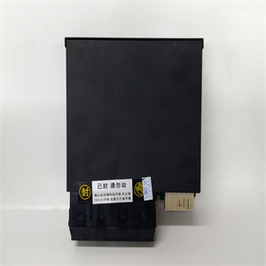


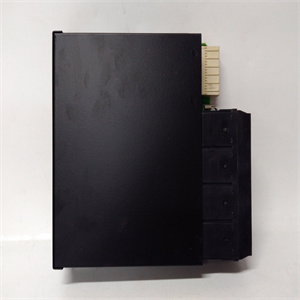
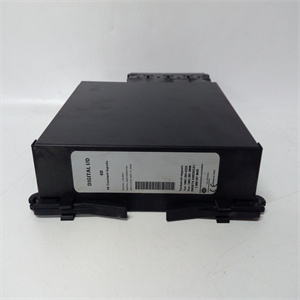
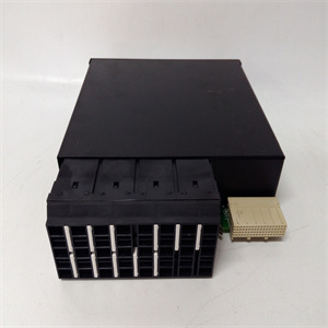
Vmivme-5588
每个计时器都有一个可独立选择的时钟源,该时钟源由“计时器x时钟选择”字段中的位模式选择,如下所示:通过将“1”写入相应的“计时器x启用”字段,可以独立启用每个计时器。类似地,通过将“1”写入适当的“timer x IRQ Enable”(定时器x IRQ启用)字段,可以独立启用每个定时器产生的中断。如果中断是由计时器生成的,则可通过读取“计时器x引起的IRQ”字段来确定中断的来源。如果该字段设置为“1”,则相应的计时器会导致中断。请注意,多个计时器可能会导致一个中断。因此,必须读取所有计时器的状态,以确保识别所有中断源。通过将“0”写入相应的“timer x Resulted IRQ”字段,可以清除特定的计时器中断。或者,写入适当的定时器x IRQ Clear(TxIC)寄存器也会清除中断。当使用“Timer x Resulted IRQ”(计时器x导致IRQ)字段清除中断时,请注意,确保使用正确的位掩码,以便不影响其他寄存器设置,这一点非常重要。清除中断的方法是使用第52页所述的“定时器x IRQ清除”寄存器。计时器控制状态寄存器2(TCSR2)计时器也由计时器控制状态寄存器2(TCSR2)中的位控制,该寄存器位于BAR2中地址的偏移量0x04处。该寄存器中的位映射如下:“读取锁存选择”位用于选择可编程定时器的锁存模式。如果该位设置为“0”,则在读取其任何一个地址时,每个计时器输出都被锁存。例如,对TMRCCR12寄存器的读取会锁存计时器1和2的计数。对TMRCCR3寄存器的读取锁存计时器3的计数。每次读取这些寄存器中的任何一个时,都会继续执行此操作。因此


Each timer has an independently selectable clock source which is selected by the bit pattern in the “Timer x Clock Select” field as follows: Each timer can be independently enabled by writing a “1” to the appropriate “Timer x Enable” field. Similarly, the generation of interrupts by each timer can be independently enabled by writing a “1” to the appropriate “Timer x IRQ Enable” field. If an interrupt is generated by a timer, the source of the interrupt may be determined by reading the “Timer x Caused IRQ” fields. If the field is set to “1”, then the respective timer caused the interrupt. Note that multiple timers can cause a single interrupt. Therefore, the status of all timers must be read to ensure that all interrupt sources are recognized. A particular timer interrupt can be cleared by writing a “0” to the appropriate “Timer x Caused IRQ” field. Alternately, a write to the appropriate Timer x IRQ Clear (TxIC) register will also clear the interrupt. When clearing the interrupt using the “Timer x Caused IRQ” fields, note that it is very important to ensure that a proper bit mask is used so that other register settings are not affected. The preferred method for clearing interrupts is to use the “Timer x IRQ Clear” registers described on page 52. Timer Control Status Register 2 (TCSR2) The timers are also controlled by bits in the Timer Control Status Register 2 (TCSR2) located at offset 0x04 from the address in BAR2. The mapping of the bits in this register are as follows: The “Read Latch Select” bit is used to select the latching mode of the programmable timers. If this bit is set to “0”, then each timer output is latched upon a read of any one of its address. For example, a read to the TMRCCR12 register latches the count of timers 1 and 2. A read to the TMRCCR3 register latches the count of timer 3. This continues for every read to any one of these registers. As a result
相关产品


