产品展示
联系我们
联系人:麦女士
手机:+86 15270269218
电话:
Q Q:3136378118
邮箱:stodcdcs@gmail.com
地址:江西省九江市瑞昌市东益路23号赛湖农商城401号
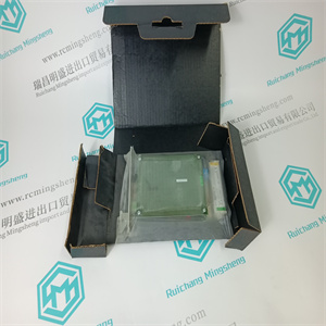

IS200BPIAG1A
光伏发电机的基本组件是光伏电池,在光伏电池中将太阳辐射转化为电流。电池由一薄层半导体材料构成,通常经过适当处理的硅,厚度约为0.3 mm,表面为100至225 cm2。硅有四个价电子(四价),通过在一个“层”上添加三价原子(例如硼-磷掺杂)和在另一个“层”上添加大量五价原子(例如磷-氮掺杂)来“掺杂”。p型区域有过多的空穴,而n型区域有过多的电子。在两层不同掺杂(P-N结)之间的接触区域中,电子倾向于从富电子半(N)移动到贫电子半(P),从而在P区域中产生负电荷的累积。电子空穴出现双重现象,在区域N中积累正电荷。因此,在结上产生电场,阻止电荷进一步扩散。通过从外部施加电压,接头仅允许电流沿一个方向流动(二极管工作)。当电池暴露在光照下时,由于光伏效应1,在N区和P区都会出现一些电偶。内部电场允许多余的电子(从材料的一部分吸收光子而来)从空穴中分离出来,并将它们推向彼此相对的相反方向。因此,一旦电子通过耗尽区,它们就不能向后移动,因为磁场阻止它们反向流动。通过将接头与外部导体连接,可以获得闭合电路,其中只要电池被照亮,电流就从具有较高电势的N层流向具有较低电势的N层。有助于提供电流的硅区域是P-N结周围的区域;电荷在遥远的地区形成,但没有电场使它们移动,因此它们重新结合。因此,光伏电池必须有一个大的表面:表面越大,产生的电流越大。5.2光伏发电厂的主要组件1当材料(通常为半导体)价带中的电子由于吸收入射到材料上的一个足够能量的光子(电磁辐射量子)而提升到导带时,会发生光伏效应。事实上,在半导体材料中,就绝缘材料而言,价电子不能自由移动,但与绝缘材料相比,价带和导带(典型的导电材料)之间的能隙很小,因此当电子从外部接收能量时,可以很容易地移动到导带。这种能量可以由光辐射提供,因此产生光伏效应。


The elementary component of a PV generator is the photovoltaic cell where the conversion of the solar radiation into electric current is carried out. The cell is constituted by a thin layer of semiconductor material, generally silicon properly treated, with a thickness of about 0.3 mm and a surface from 100 to 225 cm2 . Silicon, which has four valence electrons (tetravalent), is “doped” by adding trivalent atoms (e.g. boron – P doping) on one “layer” and quantities of pentavalent atoms (e.g. phosphorus – N doping) on the other one. The p-type region has an excess of holes, whereas the n-type region has an excess of electrons. In the contact area between the two layers differently doped (P-N junction), the electrons tend to move from the electron rich half (N) to the electron poor half (P), thus generating an accumulation of negative charge in the P region. A dual phenomenon occurs for the electron holes, with an accumulation of positive charge in the region N. Therefore an electric field is created across the junction and it opposes the further diffusion of electric charges. By applying a voltage from the outside, the junction allows the current to flow in one direction only (diode functioning). When the cell is exposed to light, due to the photovoltaic effect 1 , some electronhole couples arise both in the N region as well as in the P region. The internal electric field allows the excess electrons (derived from the absorption of the photons from part of the material) to be separated from the holes and pushes them in opposite directions in relation one to another. As a consequence, once the electrons have passed the depletion region they cannot move back since the field prevents them from flowing in the reverse direction. By connecting the junction with an external conductor, a closed circuit is obtained, in which the current flows from the layer N, having higher potential, to the layer N, having lower potential, as long as the cell is illuminated. The silicon region which contributes to supply the current is the area surrounding the P-N junction; the electric charges form in the far off areas, but there is not the electric field which makes them move and therefore they recombine. As a consequence it is important that the PV cell has a great surface: the greater the surface, the higher the generated current. 5.2 Main components of a photovoltaic plants 1 The photovoltaic effect occurs when an electron in the valence band of a material (generally a semiconductor) is promoted to the conduction band due to the absorption of one sufficiently energetic photon (quantum of electromagnetic radiation) incident on the material. In fact, in the semiconductor materials, as for insulating materials, the valence electrons cannot move freely, but comparing semiconductor with insulating materials the energy gap between the valence band and the conduction band (typical of conducting materials) is small, so that the electrons can easily move to the conduction band when they receive energy from the outside. Such energy can be supplied by the luminous radiation, hence the photovoltaic effect.
相关产品


